X-ray inspection of printed circuit boards
Non-destructive testing is one of the most popular methods for checking objects for defects. This is due to its main property, which has become its advantage – the possibility of carrying out without decommissioning the facility and stopping production, without damage and destruction, not only in specialized laboratories, but also at the location of the facility itself.
One of the methods of non-destructive testing is X-ray testing. Its essence lies in the translucence of an object with X-rays – electromagnetic radiation with a short wavelength, which allows it to penetrate even into opaque bodies.
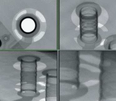
X-ray inspection of printed circuit boards is a modern and effective method for checking the installation of electronic components, which allows you to most accurately determine the presence of defects in the product, their location and size. The objects of X-ray inspection of printed circuit boards are complex boards with a high density of mounting of electronic components, electronic components on flexible boards, connectors and other parts.
The X-ray image of the object obtained during the inspection or its three-dimensional model is analyzed by a computer, and based on the data obtained, a conclusion is made about the presence of defects in the solder joints. This control is widely used due to its characteristics: reliability of testing, autonomy, maneuverability, ease of production, cost-effectiveness.
It is recommended to entrust the implementation of X-ray control of printed circuit boards to professionals – а laboratory of Non-Destructive Testing. After all, we will carry out this check promptly and provide you with the most accurate data on the presence or absence of defects in the printed circuit board.